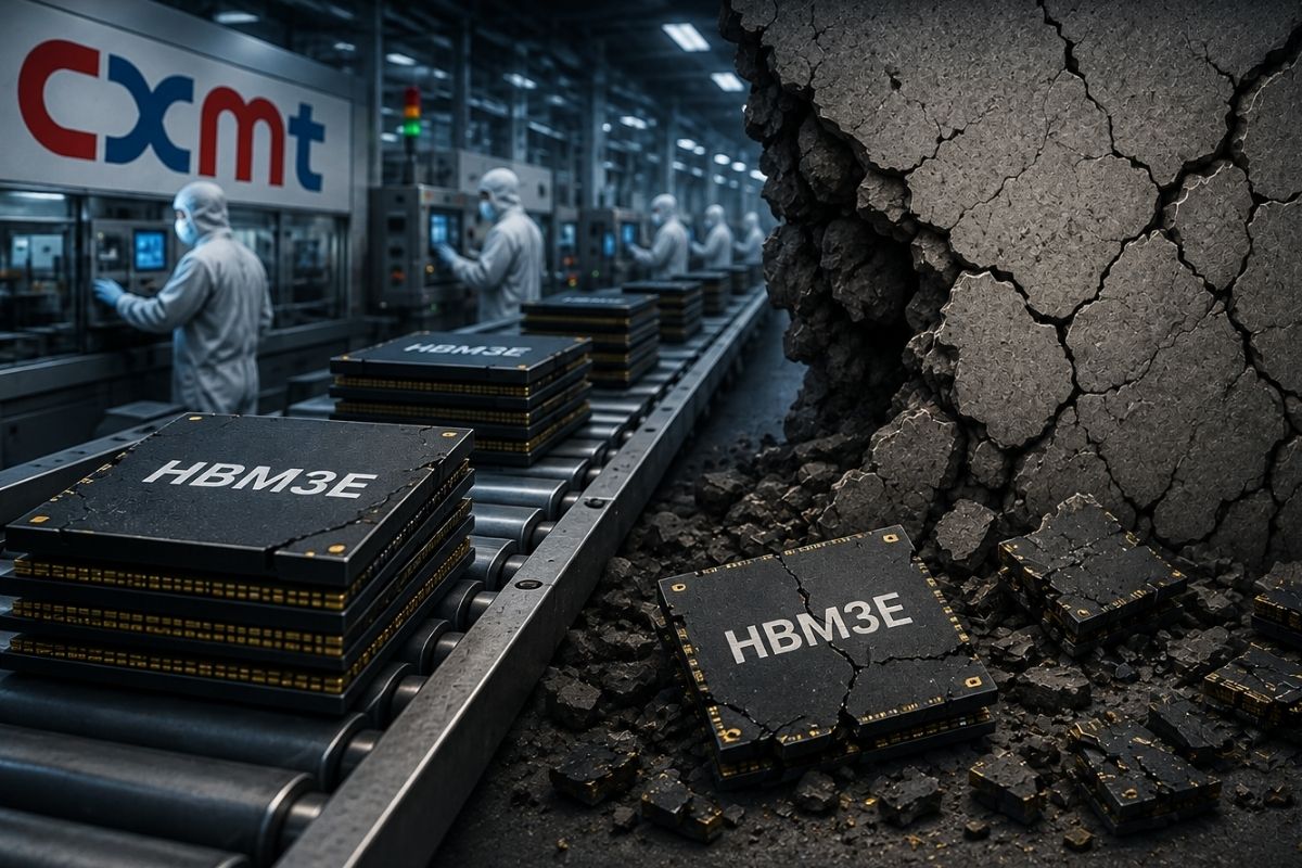
ChangXin Memory Technologies (CXMT) faces a mathematical ceiling in its push for commercial HBM3E mass production by 2027. Relying exclusively on multi-patterned deep ultraviolet (DUV) lithography caps viable die yields below 35 percent. When engineers stack these low-yield components into 8-Hi or 12-Hi memory modules, compounded error rates push final production costs up to 4.5 times higher than Western equivalents, making the hardware economically unviable without heavy state subsidies.
The SAQP Edge-Placement Bottleneck
CXMT’s memory scaling trajectory directly mirrors the throughput decay Semiconductor Manufacturing International Corporation (SMIC) encountered at its 7nm logic node. Both manufacturers rely on self-aligned quadruple patterning (SAQP) using older
ASML TWINSCAN NXT:1980Di DUV scanners to draw sub-18nm circuits.
Without access to extreme ultraviolet (EUV) systems, CXMT must expose each silicon wafer multiple times to construct advanced 1β/1γ DRAM capacitors. Every additional exposure compounds edge-placement errors.
TechInsights’ lithography overlay models indicate this cumulative misalignment restricts net commercial die yields to maximums of 35 percent.
CXMT attempts to maintain this immersion fleet using grey-market spare parts to circumvent
US Bureau of Industry and Security (BIS) export controls. However, foreign tool servicing restrictions and talent mobility friction—detailed in our coverage of
semiconductor supply-chain exit bans—prevent foreign field engineers from recalibrating sub-nanometer stage drift.
Compound Degradation in Advanced Packaging
Producing a functional DRAM die is only the baseline requirement. High-bandwidth memory architecture requires stacking eight to 12 individual dies vertically, connected by microscopic copper through-silicon vias. This packaging sequence introduces a strict mathematical penalty: final module yield equals the individual die yield raised to the power of the stacked dies, multiplied by the packaging baseline.
Applying this degradation model to DUV-processed dies reduces finished HBM3E module yields to single digits.
TrendForce supply-chain data places CXMT’s early 8-Hi HBM3 yield rate between just 10 and 25 percent. Because domestic AI accelerators—including the Ascend clusters driving the
Huawei CANN versus NVIDIA CUDA ecosystem—require massive memory bandwidth to train frontier models, these packaging yields represent the most severe constraint on Chinese AI infrastructure.
State Funding Absorbs the 4.5x Cost Multiplier
Chinese state planners maintain that custom software algorithms and DUV pitch-splitting optimizations can offset these hardware limitations. For Beijing’s strategic infrastructure, raw volume and domestic availability override cost-per-bit metrics.
The state absorbs the exorbitant cost of discarded wafers through the 344 billion yuan ($47.5 billion) third phase of the
National Integrated Circuit Industry Investment Fund. This capital allows domestic server manufacturers to bypass US sanctions, wholly separating the hardware’s strategic function from its commercial viability.
Bottom-up fab cost modeling by
SemiAnalysis calculates that accounting for extra photomask steps, extended wafer run times in DUV scanners, and high discard rates, a single CXMT HBM3E module costs 3.2 to 4.5 times more to manufacture than equivalent single-exposure EUV modules from SK Hynix or Micron. Under current physical constraints, CXMT can supply targeted domestic clusters, but cannot scale to high-volume commercial manufacturing for the open market by 2027.
Author - Presley
Updated On - October 6, 2026
Published on - September 1, 2026